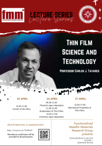
The Functionalized Metallic Materials Research Group is proud to announce a lecture series on “Thin film Science and Technology” to be delivered by Professor Carlos J. Tavares from the Physics Department of the University of Minho, Portugal.
Thin films have become an integral part of modern technology, with applications in a variety of fields including electronics, optoelectronics, energy conversion and storage. In this lecture series, Professor Tavares, a highly acclaimed expert in the field, will provide a comprehensive overview of the fundamental principles, advanced techniques, and latest developments in thin film science and technology.
The lecture series will be held at Engineering Faculty D Block, Seminar room (1st Floor) from Tuesday, April 25 to Thusday, April 27, and participation is free. However, registration is mandatory and can be done via the following link: https://tinyurl.com/ThinfilmST.
Professor Tavares (https://scholar.google.com/citations?hl=pt-PT&user=3Y24I6UAAAAJ) has an exceptional research record and extensive knowledge in thin films. He has authored more than 100 publications in leading journals and supervised numerous doctoral theses. His research interests include thin film deposition techniques, characterization, and applications in various fields.
The lecture series program is as follows:
Lecture #1: April 25 (Tuesday): 15:30-17:00
1 . Growth of thin films
1.1. Production of Thin Films: steps
1.2. The substrate surface
1.3. Film growth
i ) Condensation and nucleation of adatoms on the surface
ii ) surface mobility of adatoms
iii ) Epitaxial growth and columnar growth
- iv) Nucleation
- v) Local preferential nucleation
- vi) Volmer – Weber, Frank – Van der Merwe and Stranski – Krastanov type growth
vii ) Interface : mixing and diffusion
1.4. Morphology
i ) Thornton Model
ii ) Messier Model
Lecture #2: April 26 (Wednesday): 09:30-11:00
2 . Physical vapor deposition
2.1. History of PVD
2.2. Plasma
2.3. Sputtering
- i) Microscopic analysis of sputtering
ii ) Sputtering systems
iii ) Advantages / disadvantages of sputtering
iv ) Basic techniques of sputtering
- v) Sputtering by diode
- vi) RF Sputtering
2.4. The magnetron
i ) Schematic of a magnetron
ii ) Magnetron sputtering
iii ) Discharge plasma
iv ) Erosion on target
2.5. Interior of a deposition system
i ) Inside the magnetron
ii ) Examples of magnetrons
iii ) Advantages / disadvantages of sputtering
iv ) Bombardment
- v) Reactive Sputtering
- vi) Miniaturized Systems for sputtering
vii ) Laboratory Systems
viii ) In-line industrial systems
2.6. Sputtrering Yield
Lecture #3: April 26 (Wednesday): 11:30-12:30
3 . Evaporation of Thin Films
3.1. Evaporation Process
3.2. Growth of thin films
3.3. The implementation of the evaporation system
3.4. Evaporation sources
3.5. Materials for evaporation
Lecture #4: April 26 (Wednesday): 15:30-17:00
4 . Chemical vapor deposition
4.1. INTRODUCTION to the CVD process
4.2. Choice of a CVD system
4.3. CVD thin films for electronics
4.4. CVD processes: AP-CVD; LP -CVD ; ICP -CVD , PE -CVD , MO -CVD , HW -CVD
4.5. Applications
4.6 Atomic Layer Deposition
Lecture #5: April 27 (Thursday): 15:30-17:00
Mechanical Properties of Thin Films
- Adhesion
- Stress
- Hardness and Young Modulus
- Wear
We look forward to your participation!
